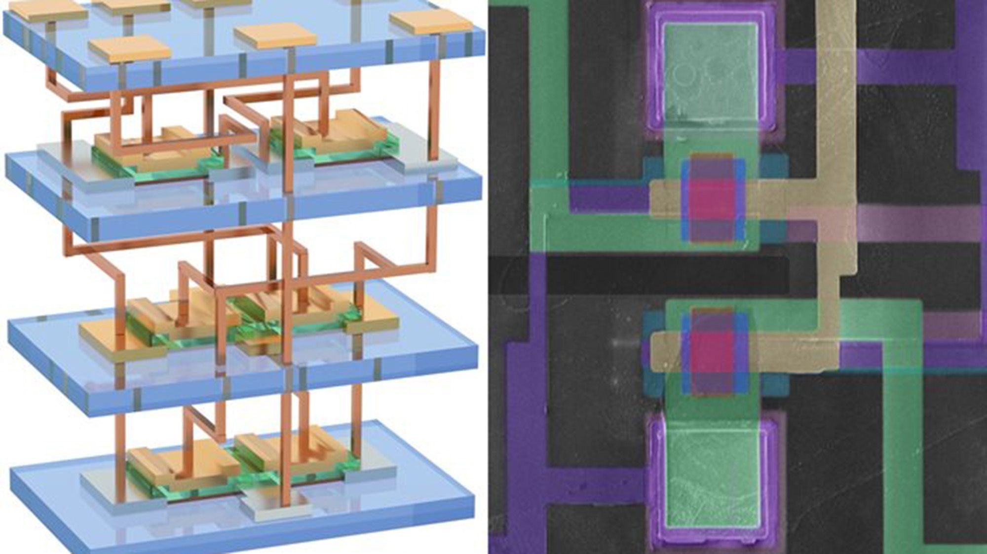
AI is hungry. It eats computing power for breakfast, lunch, and dinner, and standard flat chips can no longer feed it.
Physical limits are hitting hard. Transistors aren’t shrinking the way they used to. Not really. Not anymore. So a team at the University of Illinois did what seemed obvious in retrospect — they stacked them.
Published on May 27 in Nature, the new study details a three-dimensional silicon chip. Not a sandwich of separate chips glued together, but a single block built from ultrathin membranes.
Up is the new Out
Since the 1960S we’ve played a shrinking game. Smaller transistors meant more could fit on the same surface area. That was Moore’s law. Double the transistors every two years. Keep pushing. Keep shrinking.
It’s ending.
Qing Cao, lead author of the study, says we hit a wall of silicon itself. The intrinsic material properties. Quantum mechanics. The contacted gate pitch isn’t getting any smaller.
If you want more power you have two choices: keep squishing devices onto a flat plane until they break or build upward. Cao chose up.
Think of it like city planning. In a 2D city every bit of information needs its own six-transistor footprint. It spreads out. In a 3D city you build towers. Same function. Same bit storage. Much less floor space. And crucially, data doesn’t have to travel across miles of silicon road. It goes up a few nanometers. Faster. Cooler. Easier on the battery.
The Heat Problem
Stacking isn’t exactly new news.
The industry has tried before. Vertical integration sounds great on paper until you look at the heat.
Traditional silicon manufacturing needs 1,000 C (1,832 F) to make good chips. You cook the first layer perfect. Then you add metal wires to connect the next layer. You turn on the furnace again. Poof. The metal melts.
There’s a hard ceiling known as the “thermal budget.” After that first layer you can only handle about 400 C (752 F). Go higher and everything degrades.
Previous solutions compromised on quality. Manufacturers swapped real silicon for alternatives in the upper layers — amorphous metal oxides. Carbon nanotubes. Polycrystalline stuff. It kept the heat down but sacrificed performance and reliability. Who wants a slow chip that breaks easily?
Our method is not only easier to implement but cheaper, Cao noted. It avoids those previous pitfalls entirely.
Paper-Thin Solutions
The team at Illinois used a trick called monolithic integration. Instead of making chips separately and gluing them — which creates weak points — they build everything on one substrate.
They started with ultrathin silicon nanomemberanes. How thin? Less than 10 nanometers. Roughly the width of a single protein molecule. Compare that to a standard wafer which is half a millimeter thick. These membranes are flexible. They conform. They don’t crack under pressure.
They used a roll laminator to pick up these skins and place them on top of the base layer.
Here’s the kicker. The bond held strong at just 200 C (392 F). Five times cooler than the standard recipe. The existing metal wires survived. The silicon quality stayed high.
They made a chip with three layers. Each held 625 transistors
That number looks small. Billions exist in commercial chips right now. But this isn’t a commercial product yet. It’s a proof of concept. A prototype that shows the current flow is three to four times better than those compromise alternatives using non-silicon materials.
It works.
Now the industry has to figure out how to scale it. How to stack ten layers instead of three. How to manufacture these membranes without costing an arm and a leg. The lab result is clean. The market is messy. Will factories care enough to rebuild their lines?
That’s the next question.